The complete guide to PCB pad :types, size, spacing, repair and comparison - IBE Electronics
$ 17.99 · 5 (321) · In stock

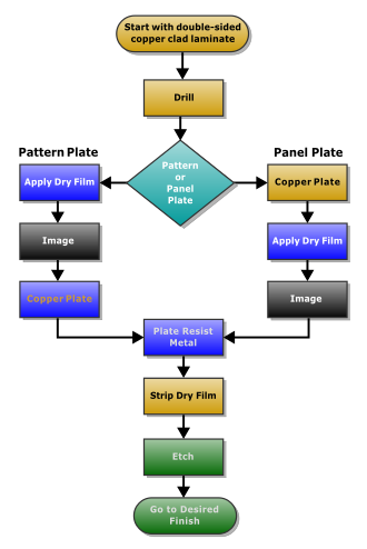
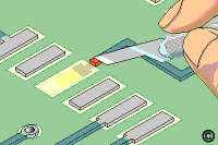
Soldering is one of the most important processes in PCBA processing. On printed circuit boards, electrical connections to all components are made via PCB pads. The PCB pads are a very critical part of the PCB that determines where components are soldered on the PCB.The size, shape, and position of pads in a PCB directly depend on the manufacturing quality of the board. Today we will take a look at the PCB pad in SMT soldering.
Soldering is one of the most important processes in PCBA processing. On printed circuit boards, electrical connections to all components are made via PCB pad.
Printed circuit board - Wikipedia
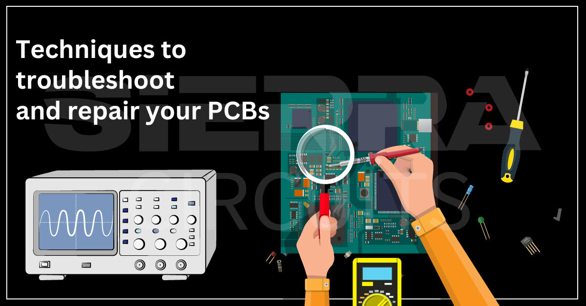
How to Troubleshoot and Repair Your PCB

Xiaomi Packs 48-megapixel Camera Into Budget Redmi Note, 55% OFF
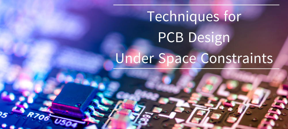
Techniques for PCB Design Under Space Constraints
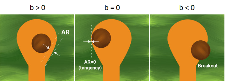
PCB Via Size and Pad Size Guidelines, Zach Peterson, Blog
How To Repair Damaged /Missing PCB Pads INVISIBLE Fix, 45% OFF
IPC-A-600: The Standard for Printed Circuit Board Inspection
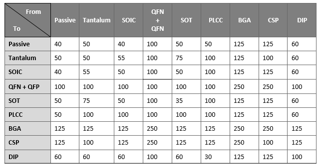
Part-to-Part, Part-to-Hole, and Part-to-Board Edge Spacing

How To Repair Damaged /Missing PCB Pads INVISIBLE Fix, 45% OFF

PCB Via Size and Pad Size Guidelines, by Raymingpcb, Feb, 2024
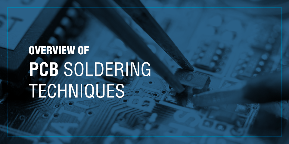
PCB Soldering Techniques What Soldering Equipment You Need